Feed linux for devices [copy] http://www.linuxfordevices.com/rss-feeds-1.xml has loading error: cURL error 22: The requested URL returned error: 404
Feed marsohod.org [copy] https://marsohod.org/component/ninjarsssyndicator/?feed_id=1&format=raw has loading error: cURL error 22: The requested URL returned error: 500
Feed Music Hackspace [copy] http://musichackspace.org/feed/rss/ has loading error: cURL error 22: The requested URL returned error: 404
Feed SparkFun Electronics [copy] http://www.sparkfun.com/feeds/news has loading error: cURL error 22: The requested URL returned error: 405
Please refrain from installing WASP-OS on new PineTimes for the moment
In July 2024, PineStore notified the community that a small hardware change was needed on the PineTime: the current flash chip was end of life (EoL) and needed to be replaced by a new one. From the software point of view, the new chip behaves exactly like the old on so very few code changes were required to support it.
Free Stuff - September 2024
The belated September 2024 recipient for the Great Scott Gadgets Free Stuff Program is Allen Paschel of Orlando, Florida in the United States. Allen is the president of The Maker Effect Foundation which exists to inspire everyone to create! The Maker Effect Foundation is a non-profit organization that runs a maker space and teaches classes at schools, libraries, and events. The maker space has CNC machines, laser etcher/cutters, 3D Printers, vacuum forming equipment, welding tools, electronic tools, and other arts tools. Soon they will be able to add software-defined radio to that list of tools as we are sending them...
Free Stuff - August 2024
The belated August 2024 recipient for the Great Scott Gadgets Free Stuff Program is Murat Sever! Murat teaches a Communication Systems Laboratory course at TOBB ETU University, Ankara, Turkey. In his labs, Murat uses two HackRFs to transmit signals of interest, which students receive via RTL-SDRs. Murat has requested an Opera Cake so his students can study Pseudo Doppler direction finding and to teach students about antenna switching and spectrum monitoring. For more information about Murat’s course, his and his students’ research projects, and their outreach programs, please check out their website (https://ele361l.github.io/).
This application for the Free Stuff program stood...
Free Stuff - July 2024
The belated July 2024 recipient for the Great Scott Gadgets Free Stuff Program is Scott Carter from Ontario, Canada! Scott operates a SETI station that uses a radio telescope he built using software defined radio. He says the radio telescope has been in operation for six and a half years, and it needs a receiver upgrade to allow scanning of frequencies above 2 GHz. We are sending Scott a HackRF One so he can make his radio telescope upgrade! Scott’s long-term goal is to make his SETI station accessible remotely for educational purposes so more folks can learn about radio...
Free Stuff - June 2024
The belated June 2024 recipient for the Great Scott Gadgets Free Stuff Program is Evan Metzinger. Evan is the president of the Cybersecurity club at Mt. San Antonio college in Walnut, California in the US. We will be sending Evan a HackRF One so he and his club can get some hands on experience with signals processing and participate in wireless capture the flag competitions.
Free Stuff - May 2024
The belated May 2024 Free Stuff recipient for the Great Scott Gadgets Free Stuff Program is Anik Mahanta from India! Anik is a student who is part of the CyRaksha Cybersecurity Club of Kolkata. CyRaksha is a free-to-join club that hosts their meetups both in-person and online. They will be using the HackRF One we are sending them to create CTF challenges, host informal meetups about RF technologies, and to create open access materials on how to use HackRF One safely while respecting Indian law.
Может ли Orange PI 5 Plus с 32 ГБ памяти заменить домашний/офисный ПК?

Производительность ARM процессоров каждый год увеличивается и все ближе к x86 процессорам. Компания Apple давно отказалась от процессоров Intel в пользу процессоров собственной разработки на ARM архитектуре. Но домашний/офисный ПК это не только процессор, но и софт, драйвера, и подключение любых устройств из коробки. Компания Shenzhen Xunlong Software вначале 2023 г. выпустила одноплатный компьютер Orange PI 5 Plus на базе высокопроизводительного процессора Rockchip RK3588 с 32 ГБ ОЗУ и возможностью подключения NVMe SSD дисков. По техническим характеристикам такой одноплатный компьютер сопоставим с домашним/офисным ПК. Проверим на сколько комфортно работать за таким одноплатником, смотреть YouTube, видео, и конечно же поиграем, установим...
Вакуумное магнетронное напыление на дому

Привет, Хабр! Последнее время здесь появились очень интересные статьи по вакуумному и стеклодувному делу, вызывающие неподдельный интерес у публики. Как насчет двинуться дальше, и начать серию статей про изготовление микросхем на дому? Многолетнюю, разумеется. Я по другому не умею :)
Тут вам и легирование кремния, и фотолитография, и вакуумное магнетронное и термическое напыление металлов и оксидов на подложку.
Совершенно случайно мне подвернулись остатки от универсального вакуумного поста ВУП-4 и я решил с головой погрузиться в эту дорогую и сложную область инженерного дела. Вообще я не планировал напылять в этой серии, но меня уговорили.
Подробности подкатомIntroducing the Omega2 Eval Boards
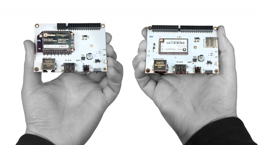
Today, we’re excited to introduce the Omega2 Eval Boards! The new Omega2 Eval Boards are built to streamline your experience with the Omega2 IoT modules – from the very first prototype to a final, production-ready device. By bringing nearly all of the Omega2’s capabilities together on a single, compact board, these Eval Boards make it easier than ever to prototype, develop, and ship your connected projects. For you, this means less time spent juggling different boards and expansions, and more freedom to focus on what matters most: bringing your ideas to life. By streamlining the entire process, the Eval Boards help you...
Support Our Work at Great Scott Gadgets
Like every open source company, Great Scott Gadgets thrives with support from you, our community. The most direct way to support us is to buy our hardware, but for folks who already have our hardware, are more interested in our software, or just want to see us grow, we have a few other options. For example, we appreciate contributions to our GitHub repositories, documentation edits, and hearing your use cases and feedback for our products and projects. If you want to know other ways you can get involved, check out our “Support our Work” page.